MEMS Packaging
MEMS packaging has been more of a challenge than packaging of conventional semiconductor devices due to its inherent characteristics. As sensors, MEMS devices are required to be exposed to the agent(s) that they are detecting. As actuators, the geometrically complex moving parts need protection. Moreover, there might be specific requirements such as optical windows, vacuum or hermetic environments. This makes MEMS especially sensitive to damage and contamination during fabrication and packaging process.
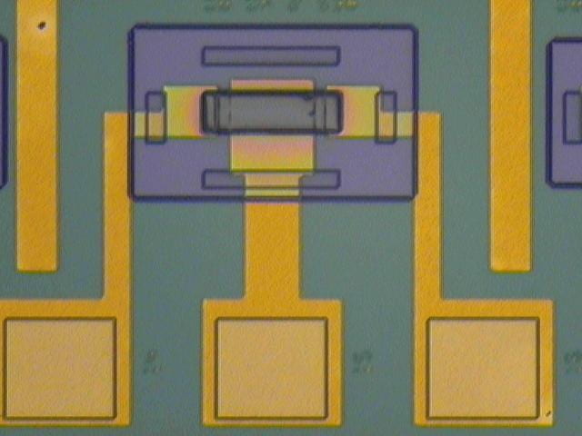
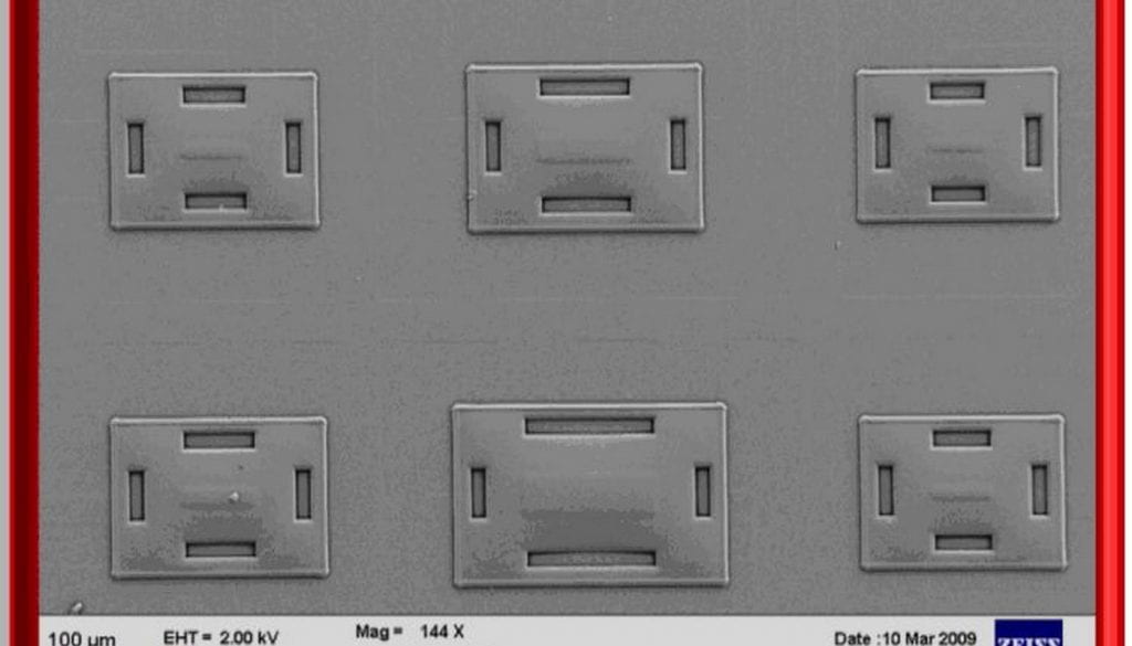
Many MEMS devices require a hermetic or vacuum operation environment. We are developing a post-CMOS compatible method for vacuum packaging of MEMS devices by growing an encapsulation layer during the device fabrication. The resulting MEMS devices are surrounded by a vacuum cavity and can then be placed in a conventional, low cost circuit package. This is a low temperature, area efficient, across wafer, device level encapsulation for MEMS devices.
Some of the recent projects are:
- Device Level Packaging of RF MEMS
- Device Level Packaging of Bolometers
Sensors
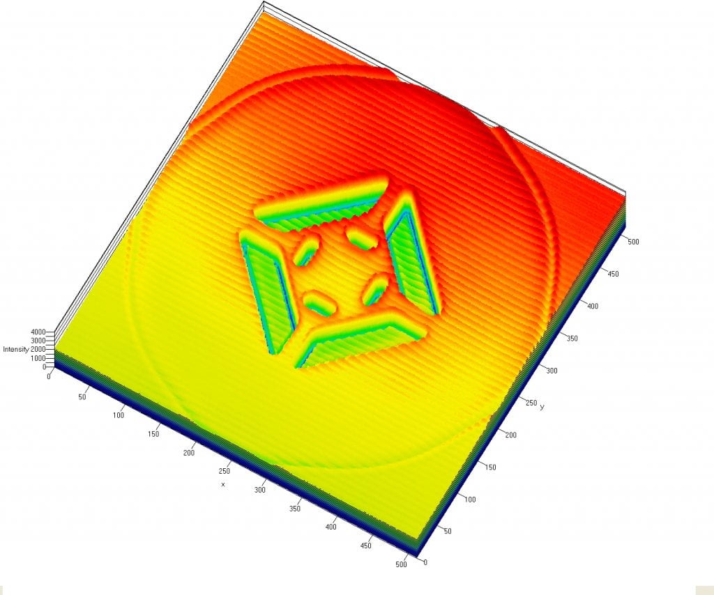
Confocal Microscop Image of a Delta Pressure Sensor
Click here to view Pressure Sensor in a capsule
The sensors research thrust area concentrates on design, fabrication, characterization and applications of
- Infrared Radiation (IR) sensors
- Temperature sensors
- Delta pressure sensors
- Absolute Pressure Sensors
- Tactile sensors
- Accelerometers
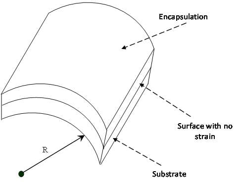
The focus is on building multifunctional sensor arrays on flexible substrates to achieve Smart Skin. Traditional electronics utilizes stiff and thick substrates where the films on top must conform to the substrate. Any stress that develops is mainly concentrated on the film. Using compliant substrates allows the bending of devices to very small radii of curvature. As shown in the figure, if the structure is bent at a radius R, the top surface (encapsulation) is under tension and the bottom surface (substrate) is under compression. If the stiffness of the electronic layer in the middle is negligible, then the electronic layer can be made to lie on a plane of no strain.
Noise & Reliability
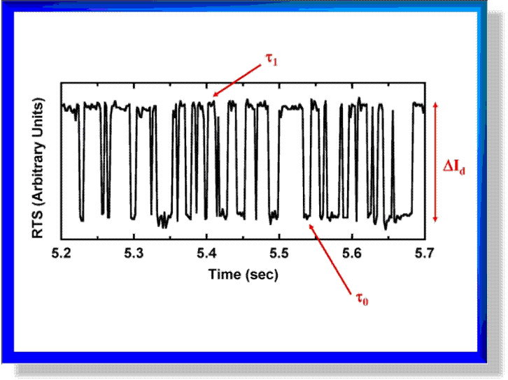
The aim of this research thrust area is to investigate the physical mechanisms behind noise and performance degradation in nanoelectronic and power electronic devices. The activities range from reliability and noise measurements under controlled degradation conditions with timed evaluation of chosen performance characteristics to analysis and modeling of the physical mechanisms causing this degradation, and eventually to prediction of device life-times.
Some of the activities of focus are:
- Noise and Noise and Random Telegraph Signals (RTS) in nanoelectronic devices
- Noise and reliability in advanced bipolar technologies
- Low-frequency noise in high-k dielectric MOSFETs:
- Noise and degradation in power MOSFETs
As new paradigms are introduced for digital information processing and analog/mixed signal applications, the group will continue to evaluate reliability and degradation mechanisms in new structures.