Nanofab
Microsensors Research
ZEYNEP CELIK & DONALD BUTLER
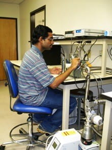
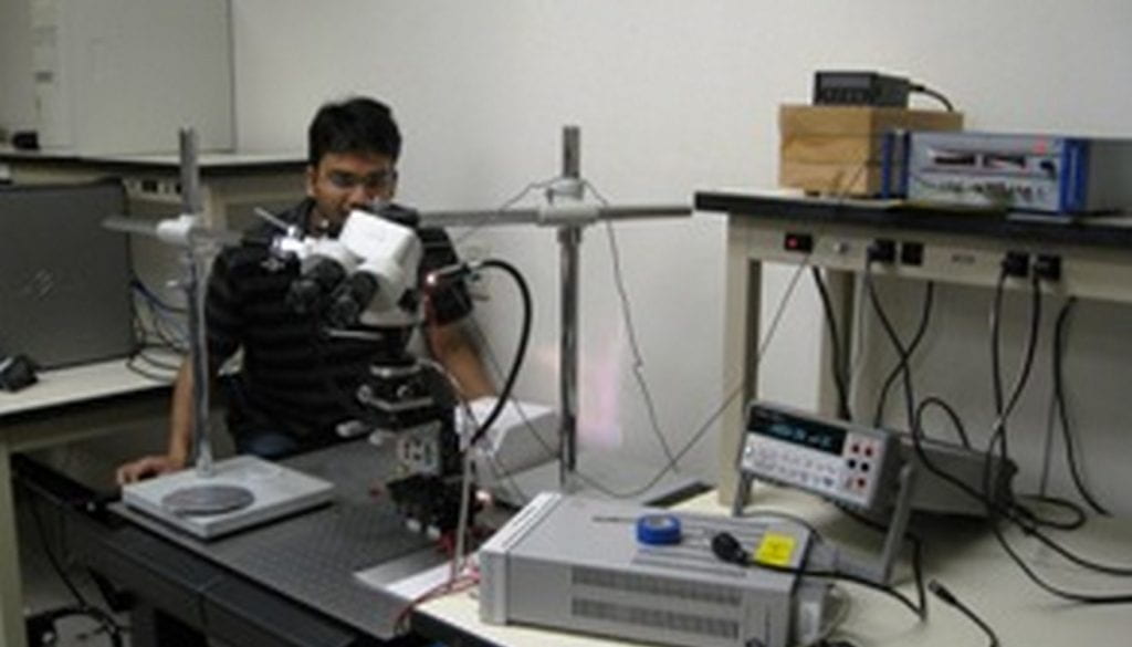
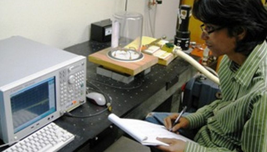
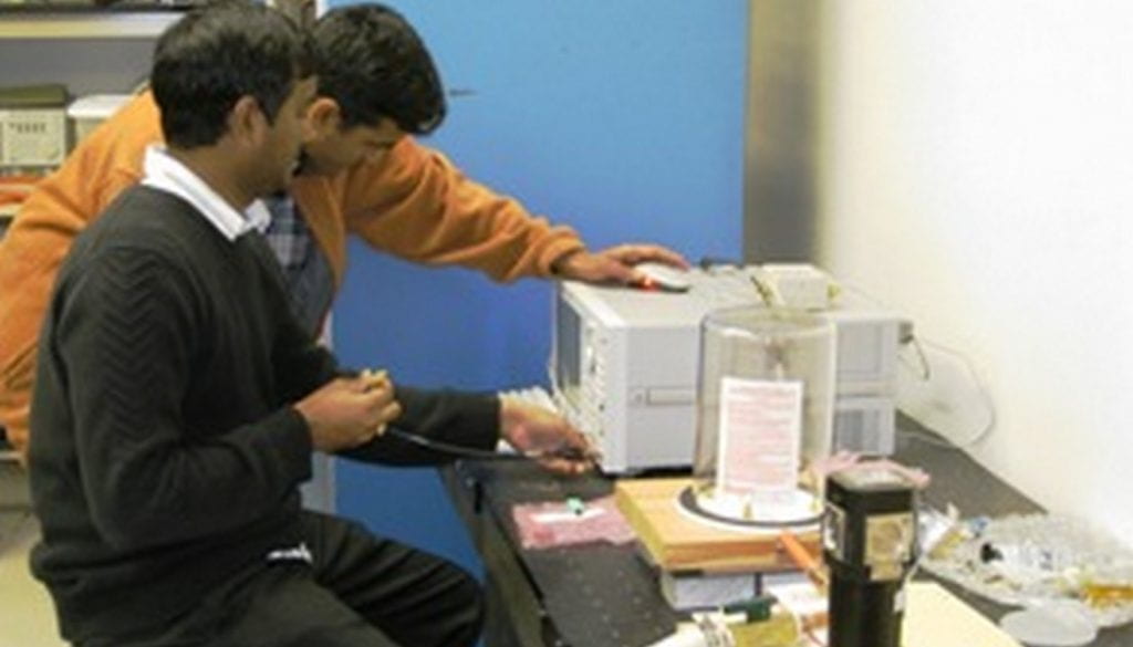
The microsensors research laboratory is used in the design, and characterization of microsensor materials and devices, including but not limited to infrared detectors, pressure and force sensors, MEMS resonators and accelerometers.
The IR radiation detector calibration set-up provides measurement capabilities from 2K to 450K temperature and from 1 – 14 µm IR wavelength. Several optical cryostats and optical tables with semiconductor characterization equipment are available in the lab.
The force/pressure sensor characterization system consists of a tensile mono-axial 10 gm load-cell with a resolution of ± 49 µN, and a customized probe-tip holder to facilitate use of probe-tips with varying radius. This is attached to a Nanopositioner with 0-50 µm Z-axis travel and a minimum resolution of 0.2 nm. A micromanipulator stage capable of moving in X, Y and Z-directions for coarse movement and a rotary tilt stage to tilt the sample from 0°-45° are utilized to hold the sample.
The accelerometer characterization setup consists of a shaker with a shaker power amplifier, a signal generator, Irvine Sensors model MS 3110 capacitive readout circuitry, and a calibrated acceleration sensor.
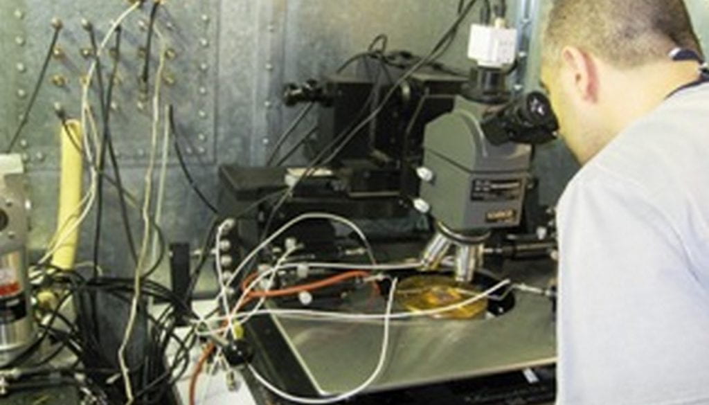
MEMS resonators are assessed in a-custom made vacuum chamber using a network analyzer, a DC power supply and vacuum pump.
Computer workstations are used as system controllers for data acquisition and modeling. Several software packages are available including ANSYS and COVENTORWARE..
Noise & Reliability
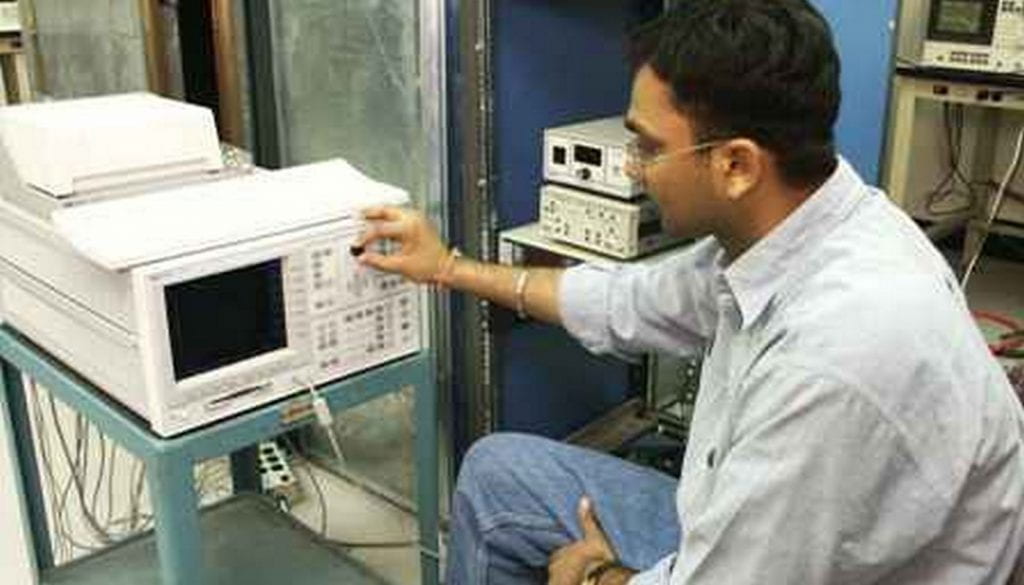
This facility is used for the characterization and modeling of solid state devices and electronic materials. The laboratory has the capability for the computerized I-V, C-V, microwave, optical, and noise characterization of devices.

Full semiconductor parameter analysis, extraction and modeling are available. Frequencies from few µHz to 4.5 GHz are covered. This lab is designed for computer controlled data acquisition and modeling.
The labs contains a 6 ft. x 6 ft. shielded room with a noise attenuation of 100 dB to electric fields and plane waves from 14 kHz to 10 GHz and 30 dB to magnetic fields at 60 Hz. A continuous flow passive cryostat in the shielded room ensures low-noise, low temperature measurements. Several shielded microprobe stations allow wafer level characterization of unpackaged devices.